Advanced Semiconductor Design
Partnering To Convert Innovation Into Silicon Solutions
Get in TouchAbout DelyanTech

Empowering Innovation in Semiconductors We are a rapidly growing semiconductor design services company, delivering end-to-end chip solutions to global leaders.
With unmatched expertise across the entire semiconductor value chain, we help our clients accelerate innovation—building next-generation products that set new benchmarks in performance, reliability, and speed-to-market.
Driven by excellence and collaboration, we transform complex ideas into cutting-edge silicon solutions that power the future.
Our Services
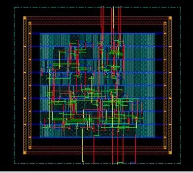
Memory, Analog, RF and full chip Layout
We specialize in end-to-end semiconductor IP development, offering deep expertise in custom memory design (SRAM, ROM, RF, Flash, DRAM), memory compilers, standard cell and I/O libraries, and analog & mixed-signal design.
Our highly skilled team delivers high-speed, high-performance analog, RF, and full-chip layouts, guiding projects seamlessly from initial concept and floor planning through to final tape-out signoff. With a strong commitment to quality, efficiency, and design excellence, we build full-chip layouts from the ground up, ensuring reliable delivery, optimized performance, and faster time-to-market for next-generation semiconductor products.
Physical Design & Signoff
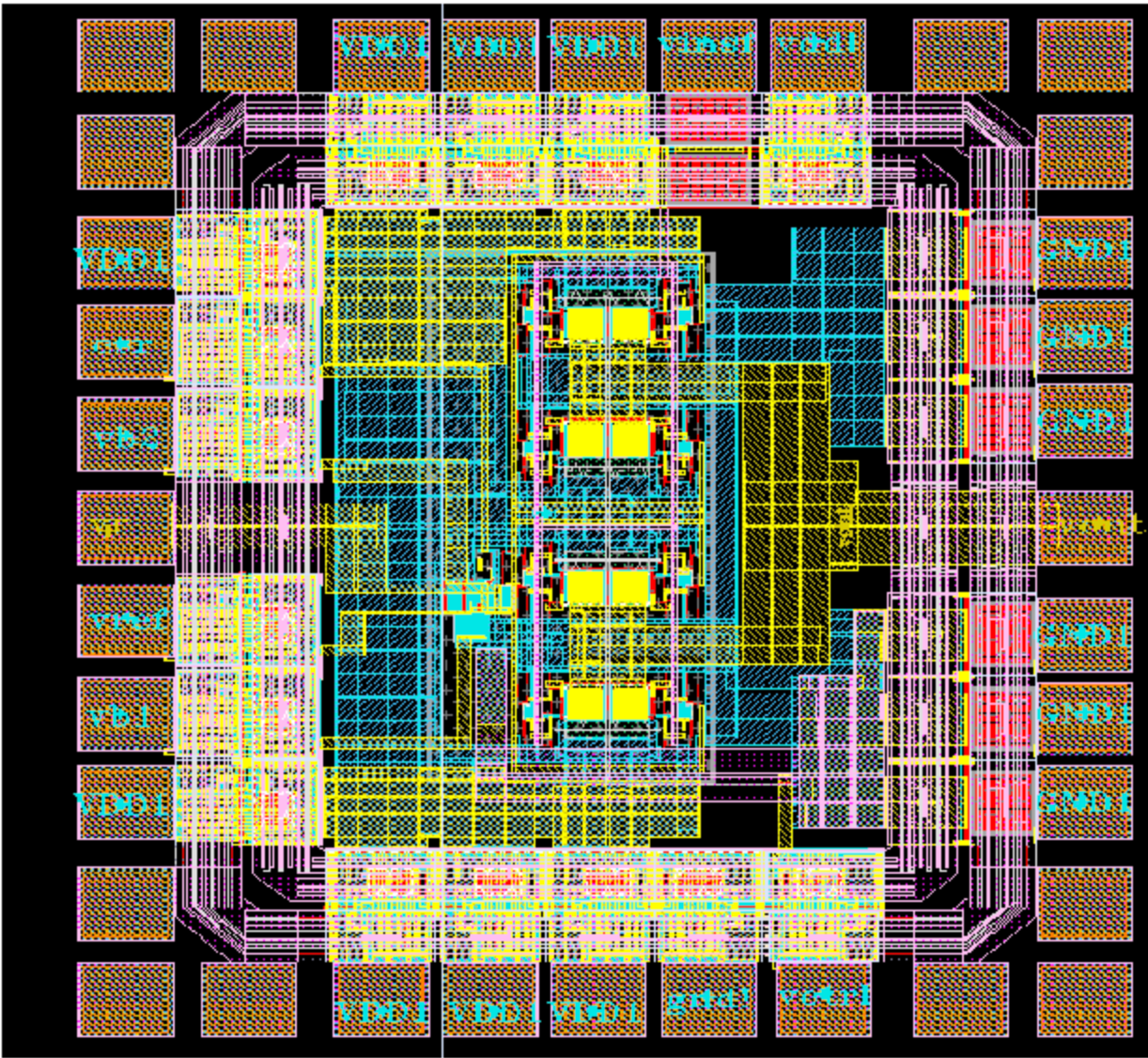
We provide end-to-end Physical Design and Signoff solutions, covering
full-chip physical design, mixed-signal and high-speed interface IPs, static timing analysis (STA), and complete design signoff. Our expertise spans technology nodes from 2nm to 180nm, enabling us to support both advanced and mature processes with precision.
We also deliver customized flow development and methodology solutions, including synthesis, place &
route (PnR), STA, and foundry-specific implementation and signoff
methodologies. With strong capabilities across the entire physical
implementation cycle, we help customers achieve high-performance,
power-efficient, area-optimized, and signoff-ready silicon, ensuring faster time-to-market and uncompromised design excellence.
ASIC, FPGA & AMS Verification Services
At DelyanTech, we offer comprehensive verification solutions that span ASIC, FPGA, and AMS designs, covering everything from IP blocks and subsystems to complete SoC/full-chip platforms. By harnessing standard methodologies, reusable verification frameworks, and intelligent automation, we empower semiconductor companies to achieve robust design validation, accelerated verification cycles, first-pass silicon success, and faster time-to-market, ensuring confidence and reliability in every product delivered.